Build note
What a logic analyser shows on an SPI bus
Part 8 built the SPI link between two chips. This part reads the same exchange on a logic analyser, which is the difference between “it seems to work” and “I can see that it works”.
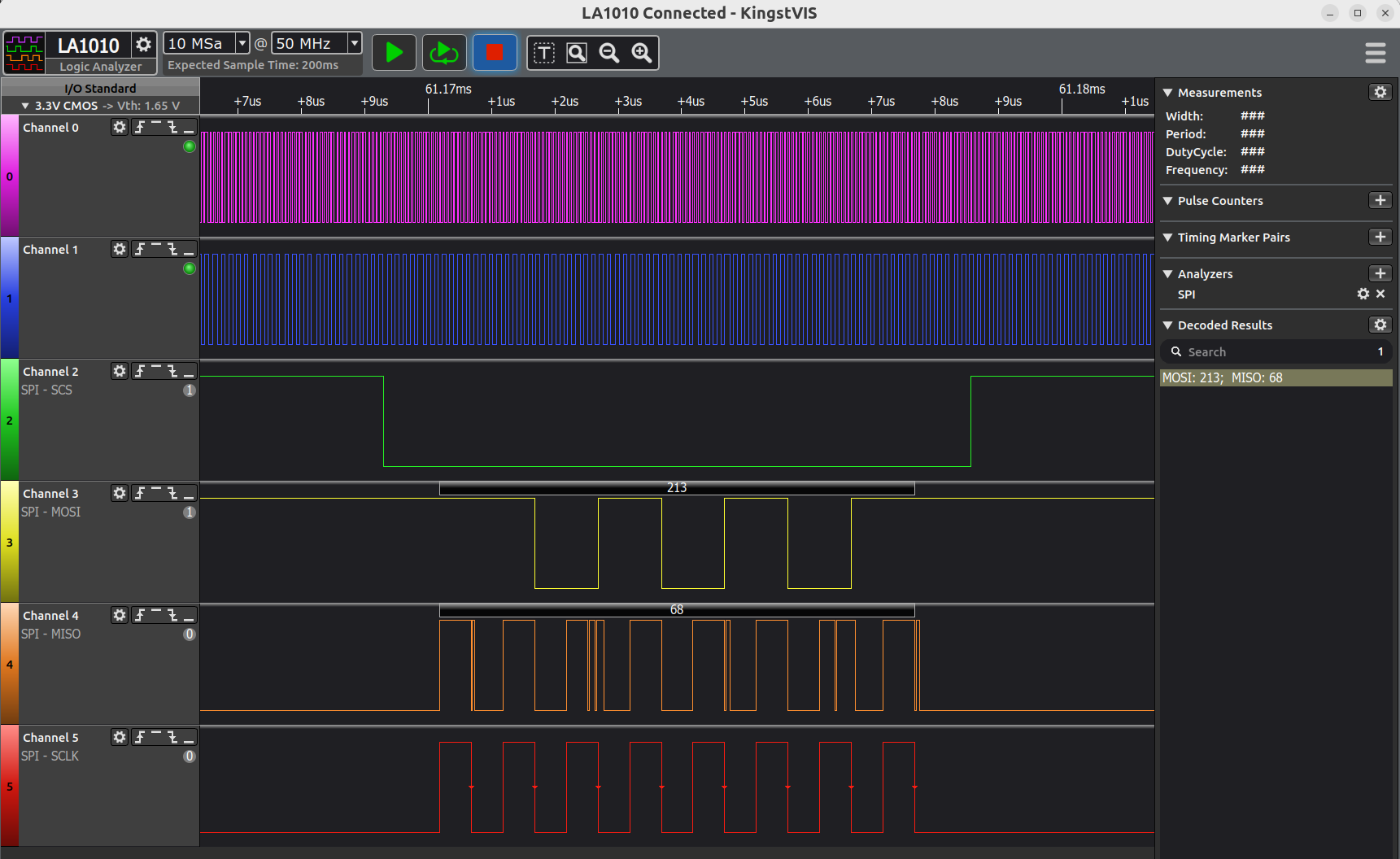
The capture below is from a Kingst LA1010 at 10 MSa/s, with four channels on the bus and two more channels left connected to unrelated signals.
Connect it properly first
- Clip the analyser ground to the same ground as both chips. Without it, every channel is measuring noise against a floating reference.
- Put one channel on
SS, one onSCK, one onMOSI, one onMISO. - Set the sample rate well above the clock. 10 MSa/s is generous for a 250 kHz SPI clock, and cheap analysers become unreliable near their limit.
- Trigger on
SSfalling. That is the only event that marks the start of a frame.
The two busy channels at the top of the capture are background activity. They are not part of the transaction, and mixing them into the decode is a common way to confuse yourself.
Read the frame in order
Chip select goes low. That is the frame boundary. Everything that matters happens while it is low.
Count the clocks. There are exactly eight. SPI has no start or stop bit, so the eighth clock is what ends the data.
Read MOSI. The decoder reports 213, which is 0xD5 or 1101 0101. The bits
are sent most significant bit first, and they are stable before each rising edge.
That timing is SPI mode 0: CPOL = 0 and CPHA = 0.
Read MISO. The analyser decodes 68, which is 0x44. The slave drove those
bits during the same eight clocks, not after them.
The detail that makes SPI click
The slave did not answer the byte it had just received. It could not. Both sides shift on the same clock edges, so the byte leaving the slave was loaded before the frame began.
That is why the master receives the value it sent one transaction earlier. In the
slave code, the interrupt reads SPDR and immediately writes it back:
ISR(SPI_STC_vect)
{
    last_rx = SPDR;
    SPDR = last_rx;
}
The line that looks like an echo is really a preload for the next frame.
Reading it without the decoder
A decoder is convenient, but you can read the frame by hand. On each rising edge
of SCK, sample MOSI and MISO. Write the bits down from the first clock to
the eighth, then convert. If the manual result disagrees with the decoder, trust
the manual one and check the decoder’s mode setting.
What a bad capture looks like
- No clocks. The master is not configured, or
SPEis off. - Clocks but no chip select. The frame never starts, so the slave ignores it.
- Nine or seven clocks. A framing or configuration error.
- MISO flat. The slave is not selected, not powered, or its
MISOpin is not an output. - Data that looks shifted by one bit. Wrong clock phase, or the slave loaded its response too late.
Why this part earns its place
A logic analyser turns a bus problem into a picture. It answers the questions that code reading cannot: is the pin actually moving, is the frame the right length, and did the other chip answer at all. Every bus in the rest of this series is easier once you can do this.
How this was made
- Written by: Rupesh, from his own SPI notes and analyser capture, with AI drafting and editing.
- Capture: Kingst LA1010, decoded in KingstVIS.
- AI-assisted sections: structure and copy editing.