Build note
Bare metal on the ATmega328P: pins, fuses and a first blink
The Arduino library is not magic. It writes the same registers, in the same order, with the same values I am about to write by hand. What it hides is the explanation. This series takes the chip on its own, on a breadboard, with no library underneath.
The first job is the smallest one: make one pin an output and turn an LED on and off. It also forces the question that catches everyone sooner or later, which is how fast the chip is actually running.
A pin is three registers
The ATmega328P groups its pins into three ports: B, C and D. Every port has the same three registers, and nothing about a pin is special until you write them.
| Register | Job |
|---|---|
DDRx |
Direction. A 1 makes that pin an output. |
PORTx |
Level. For an output, 1 drives 5 V and 0 drives 0 V. For an input, 1 turns on the pull-up. |
PINx |
The level read back from the pin. |
For Port B the register names are DDRB, PORTB and PINB, and they are at
page 72 of the datasheet.
Four lines cover almost everything you will do with a pin:
DDRB  |=  (1 << PB1);   // make PB1 an output
PORTB |=  (1 << PB1);   // drive it high
PORTB &= ~(1 << PB1);   // drive it low
PORTB ^=  (1 << PB1);   // flip it
|= adds a bit and leaves the others alone. &= ~ removes one bit. ^= flips
one. Reading 1 << PB1 as “the bit for PB1” is the whole trick.
Wiring
PB1 (chip pin 15, Arduino D9)
  |
 [220 ohm]
  |
 [LED]
  |
 GND
The chip also needs power before any of this means anything: VCC on pin 7 and AVcc on pin 20 to 5 V, ground on pins 8 and 22, a 100 nF capacitor across the supply near the chip, and a 10 k resistor from the reset pin to 5 V. If you use an external crystal, it goes across XTAL1 and XTAL2 with a 22 pF capacitor from each leg to ground.
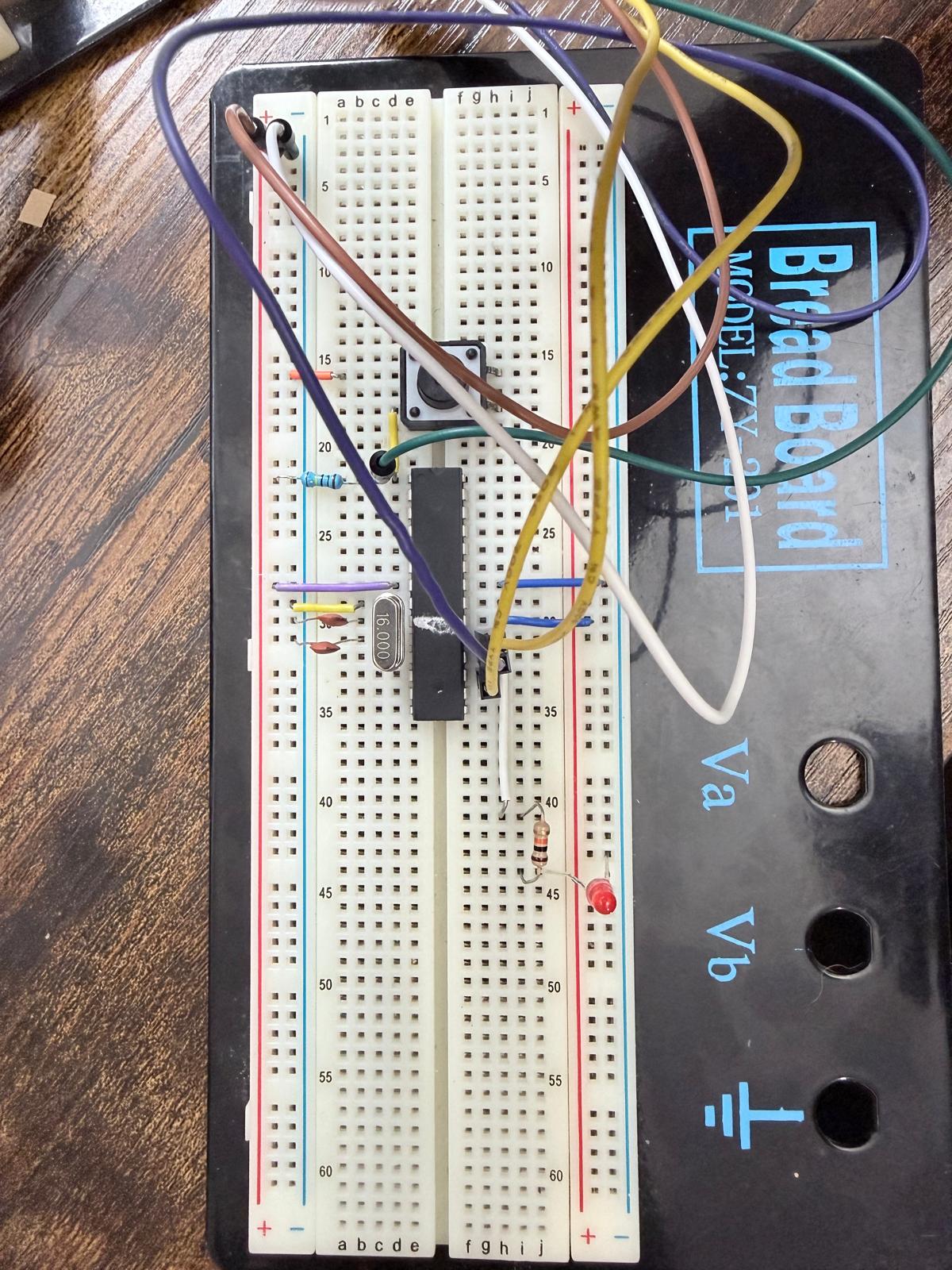
The blink
#define F_CPU 16000000UL
#include <avr/io.h>
#include <util/delay.h>

int main(void)
{
    DDRB |= (1 << PB1);

    while (1) {
        PORTB |=  (1 << PB1);
        _delay_ms(1000);
        PORTB &= ~(1 << PB1);
        _delay_ms(1000);
    }
}
Two things are easy to miss. DDRB must be set first, or the LED stays dark no
matter what PORTB says, because the output is trapped inside the chip. And
F_CPU is a promise to the delay code, not a setting for the hardware.
The clock, and the fuse that decides it
_delay_ms works out how many loop cycles to burn from F_CPU. If the number is
wrong, every delay is wrong by the same ratio. The real clock comes from the
fuse bytes, which live outside your program and are not changed when you flash
new code.
| Clock source | Low fuse | F_CPU |
|---|---|---|
| Internal RC, 8 MHz divided by 8 (factory) | 0x62 |
1000000UL |
| Internal RC, 8 MHz, no division | 0xE2 |
8000000UL |
| External crystal, 16 MHz, low power | 0xFF |
16000000UL |
| External crystal, 16 MHz, full swing | 0xF7 |
16000000UL |
The divide-by-8 bit is CKDIV8, and it is the one that catches people. The chip
is labelled 8 MHz, the factory fuse leaves the divider on, and the chip runs at
1 MHz. A 1 MHz chip with F_CPU set to 16 MHz blinks sixteen times too slowly.
The reverse mistake is worse. Set the fuse for an external crystal, forget the crystal, and the chip does not start at all. You then need a working clock source before you can talk to it again.
Read all three fuses before changing anything:
avrdude -c usbasp -p atmega328p -B 500 \
  -U lfuse:r:-:h -U hfuse:r:-:h -U efuse:r:-:h
Building and flashing
The folder has a Makefile with make, make size, make disasm, make flash
and make clean. Underneath, it is three commands:
avr-gcc -mmcu=atmega328p -Os -DF_CPU=16000000UL -c main.c -o main.o
avr-gcc -mmcu=atmega328p -o main.elf main.o
avr-objcopy -O ihex -R .eeprom main.elf main.hex
avrdude -c usbasp -p atmega328p -B 500 -U flash:w:main.hex:i
make size is worth running after every build. It prints how much of the 32 KB
flash and the 2 KB of RAM the program uses, and it is the cheapest early warning
that a buffer or an array has grown too large.
The -B 500 slows the ISP clock. Cheap programmers and long jumper wires fail
without it, usually with an unhelpful “initialization failed”.
What goes wrong first
- The LED does nothing. The pin is still an input. Check
DDRB. - It blinks at the wrong speed.
F_CPUdoes not match the fuse. - The chip will not respond. The fuse selected a clock source that is not
fitted, or the reset pin was turned into a GPIO with
RSTDISBL, which needs a high-voltage programmer to undo. avrdudecannot initialise. Check the six ISP wires, then add-B 500.- Serial output is garbage. That is Part 2’s problem, and it is almost always
a baud rate that was calculated from the wrong
F_CPU.
The habit worth keeping
Match the three things before you debug anything else: the physical clock source,
the fuse that selects it, and the F_CPU in the code. When those agree, the
timing is right and the rest of the chip becomes predictable.
How this was made
- Written by: Rupesh, from his own
c-01-atmega328pnotes and code, with AI drafting and editing. - Photo: Rupesh’s breadboard setup.
- Numbers and fuse values: from the ATmega328P datasheet and the folder’s fuse notes.
- AI-assisted sections: structure and copy editing.